Activity 3.1.1 — D Flip-Flop
Learning Objectives
By the end of this lesson, students will be able to:
- Explain the difference between combinational and sequential logic circuits
- Describe the operation of an edge-triggered D flip-flop
- Interpret and create timing diagrams for D flip-flop operation
- Identify the inputs, outputs, and operation of the 74LS74 IC
Vocabulary
Vocabulary (click to expand)
- Sequential Logic: A type of logic circuit whose output depends not only on the present value of its input signals but on the sequence of past inputs.
- Flip-Flop: A bistable multivibrator, a circuit that has two stable states and can be used to store state information.
- Clock: A signal used to synchronize the operation of sequential logic circuits.
- Rising Edge: The transition of a signal from low to high.
- Falling Edge: The transition of a signal from high to low.
- Asynchronous: Not synchronized by a clock.
Part 1: Combinational vs Sequential Logic
In previous units, we studied combinational logic. In combinational logic, the output is purely a function of the current inputs. If you change the inputs, the output changes immediately (after a tiny propagation delay).
Sequential logic is different. The output depends on both the current inputs AND the history of previous inputs. This means sequential logic has memory.
The D Flip-Flop (Data or Delay)
The D flip-flop is the most basic building block of sequential logic. It captures the value of the D-input at a specific moment (usually the rising edge of the clock) and holds that value at the Q-output until the next rising edge.
Logic Symbol and Function Table
| CLK | D | Q | Comment | | :--- | :--- | :--- | :--- | | ↑ | 0 | 0 | Reset state | | ↑ | 1 | 1 | Set state | | 0, 1, ↓ | x | Q₀ | No change (holds previous state) |
Legend: ↑ = Rising Edge, ↓ = Falling Edge, X = Don’t Care, Q₀ = Previous State
Part 2: Timing Diagrams
Timing diagrams are used to show how signals change over time. For a D flip-flop, we look at the relationship between the Clock (CLK), the Data (D), and the Output (Q).
Timing Diagram — D Flip-Flop Rising Edge Behavior
CLK: ‾‾\_\_/‾‾\_\_/‾‾\_\_/‾‾\_\_/‾‾
D:   ‾‾‾‾‾\_\_\_\_\_\_\_\_\_\_‾‾‾‾‾‾
Q:   \_\_\_\_‾‾‾‾‾‾\_\_\_\_\_\_\_\_
Key pattern: Q changes ONLY on the rising edge of CLK. When CLK rises and D=1, Q goes HIGH. When CLK rises and D=0, Q goes LOW. Between edges, Q holds its value regardless of D.
Part 3: Interactive Practice
D Flip-Flop Timing Diagram
Toggle D to set the data input, then press Clock Pulse to trigger a rising edge. Watch Q capture D at each edge. Between edges, Q holds steady — changes to D are ignored.
Use the timing diagram above to trace through the behavior. For each rising edge of CLK, check the value of D — that becomes the new value of Q.
Part 4: Edge-Triggered vs Level-Triggered
D flip-flops are edge-triggered, meaning they only respond to the transition of the clock signal.
Key insight: Edge-triggering prevents “race conditions” where an output might change multiple times within a single clock pulse.
Part 5: The 74LS74 Dual D Flip-Flop IC
The 74LS74 is a popular IC containing two independent D flip-flops. It also includes asynchronous Preset (PR) and Clear (CLR) inputs.
- Asynchronous inputs override the clock.
- Preset sets Q to 1.
- Clear resets Q to 0.
- Both PR and CLR on the 74LS74 are active-low (indicated by the circle on the symbol or the bar over the name).
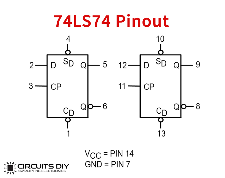
Pinout Diagram
┌─────────────────────┐
1D ┤ 1 14 ├─ VCC
1CLK ┤ 2 74LS74 13 ├─ 2CLR'
1PRE ┤ 3 12 ├─ 2PRE'
1Q ┤ 4 11 ├─ 2CLK
1Q' ┤ 5 10 ├─ 2D
GND ┤ 6 9 ├─ 2Q
  ┤ 7 8 ├─ 2Q'
└─────────────────────┘
Pin Description
| Pin | Function | | :--- | :--- | | 1D, 2D | Data inputs | | 1CLK, 2CLK | Clock inputs (rising edge triggered) | | 1PRE’, 2PRE’ | Asynchronous preset (active LOW) | | 1CLR’, 2CLR’ | Asynchronous clear (active LOW) | | 1Q, 2Q | Normal outputs | | 1Q’, 2Q’ | Complementary outputs |
Part 6: Building a D Flip-Flop Circuit
Components
| Component | Quantity | | :--- | :--- | | Breadboard | 1 | | 74LS74 IC | 1 | | LED | 1 | | 330 ohm resistor | 1 | | Push button (SPST) | 2 | | Jumper wires | As needed | | +5V power supply | 1 |
Circuit Connections
- Power: Connect VCC (pin 14) to +5V, GND (pin 7) to GND.
- Data Input: Connect a toggle switch to pin 2 (D input).
- Clock: Connect a push button to pin 3 (CLK).
- Outputs: Connect pin 5 (Q) to an LED with a resistor to ground.
- Stability: Tie PRE’ (pin 4) and CLR’ (pin 1) to +5V to prevent random triggering.
Part 7: Practice Problems
Problem 1 — Predict the Output
Given the following D input and clock waveforms, draw the Q output waveform. Assume Q starts at 0.
Show Solution
CLK: __‾‾__‾‾__‾‾__‾‾
D:   ‾‾‾‾‾‾________
Q:   ____‾‾‾‾____
Explanation:
- Initial Q = 0.
- At first rising edge: D = 1, so Q becomes 1.
- D changes to 0 between edges, but Q holds.
- At second rising edge: D = 0, so Q becomes 0.
Summary
- Sequential logic has memory (output depends on current inputs AND previous state).
- D flip-flops store one bit of data, capturing D at the clock edge.
- Edge-triggered devices only change on clock transitions, not levels.
- The 74LS74 is a common IC with two independent D flip-flops and asynchronous active-low controls.
Custom activity — adapted from PLTW Digital Electronics