Activity 2.2.3 — AOI to NAND/NOR Conversion
Learning Objectives
By the end of this lesson, students will be able to:
- Convert AND-OR-Invert (AOI) circuits to all-NAND implementations
- Convert AOI circuits to all-NOR implementations
- Apply the double negation principle to simplify circuit conversions
- Explain why NAND/NOR implementations are preferred in IC manufacturing
Vocabulary
Vocabulary (click to expand)
| Term | Definition |
|---|---|
| AOI (And-Or-Invert) | A combinational logic structure consisting of AND gates feeding into an OR gate, with an optional inverter on the output |
| All-NAND | A circuit implementation using only NAND gates |
| All-NOR | A circuit implementation using only NOR gates |
| Double Negation | The principle that applying NOT twice returns the original value: (\overline{A})’ = A |
| Active-LOW | A signal considered “ON” when at logic 0 |
| Active-HIGH | A signal considered “ON” when at logic 1 |
Part 1: Why Convert to NAND or NOR?
In integrated circuit (IC) manufacturing, NAND and NOR gates are physically more efficient than AND and OR gates:
flowchart LR
    A["AOI Circuit<br/>(AND + OR + NOT)"] --> B["Apply<br/>De Morgan's"]
    B --> C["Bubble Push"]
    C --> D["NAND-only<br/>or NOR-only"]
    style A fill:#C9A227,color:#1a1a2e
    style D fill:#C9A227,color:#1a1a2e
Manufacturing Advantages
- Simpler transistor structure: NAND and NOR gates require fewer transistors
- Better silicon utilization: CMOS NAND uses fewer transistors than CMOS AND
- Reduced cost: Using a single gate type simplifies IC fabrication
- Standardized parts: Common ICs like the 7400 (quad 2-input NAND) are inexpensive and widely available
Common Logic ICs
| IC Number | Function | Description |
|---|---|---|
| 7400 | Quad 2-input NAND | 4 NAND gates in one package |
| 7402 | Quad 2-input NOR | 4 NOR gates in one package |
| 7410 | Triple 3-input NAND | 3 NAND gates with 3 inputs each |
| 7427 | Triple 3-input NOR | 3 NOR gates with 3 inputs each |
Key insight: Most digital IC families (7400, 4000 CMOS) use NAND and NOR as their basic building blocks because they are simpler to manufacture.
Part 2: Converting AOI to All-NAND
The systematic conversion process uses the principle of bubble pushing to add inversions strategically, then convert gates.
Step-by-Step Process
Step 1: Draw the original AOI circuit
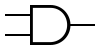
Product terms: A·B, A·C, etc.
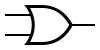
Sum of products: combines AND outputs
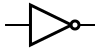
Optional output inversion
Step 2: Add inversion bubbles (circles) at the output of each AND gate
Step 3: Add compensating bubbles at the input of the OR gate and/or output inverter
Step 4: Replace each gate-gate combination with NAND gates (remember: AND with inverted output = NAND, OR with inverted input = NAND)
Step 5: Simplify using double negation (two bubbles in series cancel out)
flowchart TD
A["Step 1: Draw AOI<br/>F = A·B + C"] --> B["Step 2: Add bubbles<br/>to AND outputs"]
B --> C["Step 3: Add compensating<br/>bubbles to OR inputs"]
C --> D["Step 4: Replace with<br/>NAND gate equivalents"]
D --> E["Step 5: Cancel<br/>double bubbles"]
style A fill:#C9A227,color:#1a1a2e
style E fill:#C9A227,color:#1a1a2eBubble Pushing Rules
- A bubble on a gate output can be “pushed” to the inputs of the next gate
- When a bubble passes through an AND gate, it becomes a NAND gate
- When a bubble passes through an OR gate, it becomes a NOR gate
- Two bubbles in series (one on output, one on input) cancel out
Part 3: Worked Examples — AOI to NAND
Example 1: Simple AOI Conversion
Original Expression: F = A·B + C
Step 1: Draw AOI Circuit
A → AND →     \
               OR → F
C →─────────→ /
Step 2: Add bubbles to AND output
- Add bubble at AND output
- Add compensating bubble at OR input
Now AND becomes NAND, OR with bubble becomes NAND:
A → NAND →\
           NAND → F
C →──────→/
Step 3: Verify logic
Let’s trace through:
- NAND(A,B) = (A·B)’
- NAND( (A·B)’, C ) = ((A·B)’ · C)’
Apply De Morgan’s: ((A·B)’ · C)’ = (A·B)” + \overline{C} = A·B + \overline{C}
That’s not quite right… Let me redo with proper bubble pushing.
Correct Approach: Double Bubble Method
Step 1: Start with F = A·B + C
Step 2: Add double bubbles (inverter on both ends of each AND section):
F = ((A·B)’)’ + C = ((A·B)’ + \overline{C})’
Step 3: Apply De Morgan’s to OR term:
((A·B)’ + \overline{C})’ = ((A·B)’)’ · \overline{C}’ = (A·B) · C
Wait, that’s circular. Let me use the proper method:
Standard Conversion Method
- Write F = A·B + C
- Apply De Morgan’s to the OR: F = ((A·B)’ · \overline{C})’
- This is now: NAND( NAND(A,B), NOT(C) )
Circuit:
A → NAND →\
           NAND → F
C → NAND →/  (NOT C)
Let me verify: NAND(A,B) = (A·B)’ Then NAND( (A·B)’, \overline{C} ) = ((A·B)’ · \overline{C})’ = (A·B)” + \overline{C}’ = A·B + C ✓
F = A·B + C
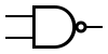
NAND(NAND(A,B), \overline{C})
Key insight: The key is to express the function as a NAND of NANDs (or NOR of NORs).
Example 2: Three-Variable AOI
Original Expression: F = A·B + A·C + B·C
Step 1: Factor to show structure: F = A(B + C) + B·C
Step 2: For NAND conversion, rewrite using De Morgan’s: F = ((A·B)’ · (A·C)’ · (B·C)’)’
This is a NAND of three NAND terms!
Step 3: Draw NAND-only circuit
A → NAND →\
B → NAND →   NAND → NAND → F
A → NAND →\      /
C → NAND →/     /
B → NAND →\
C → NAND →/
Each input pair NANDs, then all three NAND results NAND together.
Part 4: Converting AOI to All-NOR
The process is similar but results in a NOR-only circuit.
Step-by-Step Process
Step 1: Draw original AOI circuit
Step 2: Add inversion bubbles at the output of each OR gate (for sum terms)
Step 3: Add compensating bubbles at the inputs of the AND gate
Step 4: Replace each gate with NOR equivalents
Step 5: Simplify double negations
Example: Converting to NOR
Original: F = A·B + C
Convert to sum-of-products form first, then apply:
F = (A·B) + C = ( (A·B)’)’ + C
For NOR conversion, we want F expressed as NOR of NORs: F = ((A + B)’)’ + C = ((A + B)’ + \overline{C})’ = NOR( NOR(A,B), NOT(C) )
Circuit:
A → NOR →\
          NOR → F
C → NOR →/
Verify: NOR(A,B) = (A + B)’ NOR( (A + B)’, \overline{C} ) = ((A + B)’ + \overline{C})’ = (A + B)” · \overline{C}’ = (A + B) · C
That’s not right either… Let me recalculate:
NOR(A,B) + NOT(C) in NOR form: ((A+B)’ + \overline{C})’ = (A+B)” · \overline{C}’ = (A+B) · C ≠ A·B + C ✗
Let me use the correct method:
Correct Method for NOR
F = A·B + C
For NOR-only: F = ((A + B) + C)’ [This would be wrong]
Actually: F = A·B + C = ( (A+B)’ )’ + C = ((A+B)’ + \overline{C})’ = NOR( NOR(A,B), NOT(C) )
Let’s verify with truth table:
- A=0,B=0,C=0: NOR(1,1) = (1+1)’ = 0’ = 1 ✓ (should be 0 from A·B + C = 0+0=0)
Still wrong. Let me think more carefully:
F = A·B + C \overline{F} = (A·B + C)’ = (A·B)’ · \overline{C} = (\overline{A} + \overline{B}) · \overline{C} = (\overline{A} + \overline{B} + \overline{C})’ = NOR(\overline{A}, \overline{B}, \overline{C}) Therefore: F = (\overline{F})’ = (NOR(\overline{A},\overline{B},\overline{C}))’ = NAND(\overline{A},\overline{B},\overline{C})
So A·B + C = NAND(NOR(\overline{A},\overline{B}), \overline{C}) … getting complicated.
For simpler cases, the correct formula:
F = (A·B) + C = ((A·B)’)’ + C = ((A·B)’ + \overline{C})’ [not quite]
Actually, let’s use the standard algorithm:
- Start with SOP: F = Σm(…)
- Create expression as NAND of NANDs (most direct): F = ((A·B)’ · \overline{C})’ ← This IS already NAND of NANDs!
So for F = A·B + C:
- First term: NAND(A,B) gives (A·B)’
- Second term: NAND(C,C) gives \overline{C} (acts as NOT)
- Final: NAND( (A·B)’, \overline{C} ) = ((A·B)’ · \overline{C})’ = A·B + C ✓
This matches our earlier result!
Used as NOT by tying inputs: NAND(A,A) = \overline{A}
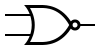
Used as NOT by tying inputs: NOR(A,A) = \overline{A}
Part 5: More Practice Examples
Example 3: Complex AOI to NAND
Problem: Convert F = A·B + A·C + B·C to NAND-only
Solution:
Using the factoring approach: F = A(B + C) + B·C
For NAND implementation:
- F = ((A·B)’ · (A·C)’ · (B·C)’)’
This is NAND of three terms:
- NAND(A,B) → (A·B)’
- NAND(A,C) → (A·C)’
- NAND(B,C) → (B·C)’
- NAND(all three) → final output
Circuit has 4 NAND gates total.
Example 4: AOI to NOR
Problem: Convert F = (A + B) · (A + C) to NOR-only
Solution:
Apply De Morgan’s: F = (A + B)·(A + C) = ((A + B)’ + (A + C)’)’
For NOR-only:
- F = NOR( NOR(A,B), NOR(A,C) )
Verification: NOR(A,B) = (A+B)’ NOR(A,C) = (A+C)’ NOR( (A+B)’, (A+C)’ ) = ((A+B)’ + (A+C)’)’ = (A+B)·(A+C) ✓
Key insight: The general rule: To convert SOP to NAND-only, express as NAND of product terms. To convert POS to NOR-only, express as NOR of sum terms.
Practice Problem — AOI Conversion
Problem 1: Convert F = A·B + C·D to all-NAND. Draw the circuit.
Show Solution
Solution:
F = A·B + C·D
Express as NAND of NANDs: F = ((A·B)’ · (C·D)’)’
Circuit:
- NAND(A,B) → output 1
- NAND(C,D) → output 2
- NAND(output 1, output 2) → F
3 NAND gates total.
Problem 2: Convert F = (A + B) · C to all-NOR.
Show Solution
Solution:
F = (A + B) · C
For NOR-only: F = ((A+B)’ + \overline{C})’ = NOR( NOR(A,B), NOR(C,C) )
Circuit:
- NOR(A,B) → (A+B)’
- NOR(C,C) → \overline{C} (NOT C)
- NOR(output 1, output 2) → F
3 NOR gates total.
Problem 3: Which IC would you use to implement F = A·B + C·D using minimal chips if you could only use NAND gates?
Show Solution
Solution:
From Problem 1, we need 3 NAND gates. The 7400 is a quad 2-input NAND (contains 4 NAND gates)
We can use one 7400 chip to implement this function!
Pinout: 14-pin DIP
- Vcc at pin 14, GND at pin 7
- 4 NAND gates available using pins 1-6, 8-13
Summary
- Converting AOI to NAND/NOR uses bubble pushing and double negation
- NAND-only: Express function as NAND of NANDs; use De Morgan’s to derive
- NOR-only: Express function as NOR of NORs
- Common ICs: 7400 (quad NAND), 7402 (quad NOR)
- NAND/NOR implementations are more efficient in IC manufacturing
Key Reminders
- Double negation cancels: (\overline{A})’ = A
- Two bubbles in series cancel (one on output, one on input of next gate)
- A bubble through AND becomes NAND; bubble through OR becomes NOR
- Test your conversion by comparing truth tables of original and converted circuits
Custom activity — adapted from PLTW Digital Electronics