Activity 2.1.3 — AOI Circuit Implementation
Learning Objectives
By the end of this lesson, students will be able to:
- Convert a Boolean expression into a logic circuit diagram
- Derive SOP expressions from truth tables and implement them as AOI circuits
- Identify and use common 74-series TTL integrated circuits (7408, 7432, 7404)
- Wire a simple combinational logic circuit on a breadboard
- Test a circuit by verifying truth table entries match actual outputs
- Draw circuit diagrams using proper gate symbols and signal flow
Vocabulary
Vocabulary (click to expand)
| Term | Definition |
|---|---|
| Circuit Implementation | The process of building a logic circuit from a given Boolean expression or truth table |
| Breadboard | A prototyping board with connected rows and columns for temporarily wiring circuits without soldering |
| 74-Series IC | A family of standardized TTL integrated circuits (Transistor-Transistor Logic) with specific functions |
| Pinout | A diagram showing the physical layout of pins on an integrated circuit |
| Flyback Wires | Short wires used to connect separate sections of a breadboard or route signals |
| VCC | The positive power supply voltage (+5V for TTL logic) |
| GND | Ground reference (0V) connection |
| Fan-out | The number of gate inputs a single output can drive without malfunction |
Part 1: From Expression to Circuit
Implementation is the reverse of analysis. Given a Boolean expression, you must draw the logic circuit that produces it. Given a truth table, you first convert it to SOP form, then draw the circuit.
The Implementation Process
flowchart LR
    TT["Truth Table"] --> SOP["SOP Expression\n(from minterms)"]
    SOP --> AND["AND Gates\n(one per product term)"]
    AND --> OR["OR Gate\n(combine terms)"]
    OR --> CIR["Complete Circuit"]
Given an expression: $Z = AB + CD$
Step 1: Identify the operations
- $AB$ is an AND operation
- $CD$ is an AND operation
- The + means OR
- The expression is: (A AND B) OR (C AND D)
Step 2: Draw AND gates first
- Draw one AND gate for AB
- Draw a second AND gate for CD
Step 3: Draw the OR gate
- Connect outputs of both AND gates to the OR gate
- The OR gate output is Z
Step 4: Connect inputs
- Inputs A and B go to the first AND gate
- Inputs C and D go to the second AND gate
Resulting Circuit:
A ----+\    _____
      | +--|     \
B ----+  (AND)    \    _____
               +---+--|     \
                   |  | OR    )--- Z
               +---+--|_____/
                   |
C ----+\    _____/ |
      | +--|     \ |
D ----+  (AND)    |
      +--|_____/
Key insight: Always work from the “inside out.” Identify the innermost operations first, draw those gates, then connect to gates for outer operations. In $Z = AB + CD$, the AND operations are inside, so draw them first.
Part 2: Worked Examples
Worked Example 1 — Simple SOP Implementation
Expression: $Z = \overline{A}B + A\overline{B}$
Step 1: Identify operations
- $\overline{A}B$: NOT A AND B
- $A\overline{B}$: A AND NOT B
- Final: OR of the two terms
Step 2: Draw the circuit
A ----+
      (|)
      |  +----+\    _____
      +--|     \  |     |
      |  | AND   )-+---\ |
B ----+--|_____/  |   | |    _____
                |   +-+--|     \
                +------| AND   )--- Z
                |   +-+--|_____/
      +---------+---| |
      |         |   | |
      |   ____/ |   | |
      |  /      +---+ |
      | /             |
C ----+/              |
      (|)             |
      +---------------+
Simplified steps:
- Invert A → $\overline{A}$
- Invert B → $\overline{B}$
- AND $\overline{A}$ with B
- AND A with $\overline{B}$
- OR the two results
Worked Example 2 — Multi-Level Implementation
Expression: $Z = (A + B)(C + D)$
Step 1: Identify operations (inside parentheses first)
- $A + B$: OR operation
- $C + D$: OR operation
- Final: AND of the two OR results
Step 2: Draw the circuit
A -----+
       |   _____
B -----+--|     \   +----+\    _____
       +--| OR    )--+   |   |     |
          |_____/     +---| AND   )--- Z
C ----------+   +---------|_____|
       |   _______   +--+
D -----+--|     \   |
       +--| OR    )--+
          |_____/
Process:
- Draw first OR gate for A + B
- Draw second OR gate for C + D
- Connect both outputs to AND gate
- AND output is Z
Worked Example 3 — From Truth Table to Circuit
Truth Table:
| A | B | Z |
|---|---|---|
| 0 | 0 | 0 |
| 0 | 1 | 1 |
| 1 | 0 | 1 |
| 1 | 1 | 0 |
Step 1: Write SOP expression
- Row 1: A=0, B=1, Z=1 → minterm: $\overline{A}B$
- Row 2: A=1, B=0, Z=1 → minterm: $A\overline{B}$
$$Z = \overline{A}B + A\overline{B}$$
Step 2: Draw the circuit
- Invert A → $\overline{A}$
- Invert B → $\overline{B}$
- AND $\overline{A}$ with B
- AND A with $\overline{B}$
- OR the results
Step 3: Verify truth table
- A=0, B=0: $Z = (1)(0) + (0)(1) = 0 + 0 = 0$ ✓
- A=0, B=1: $Z = (1)(1) + (0)(0) = 1 + 0 = 1$ ✓
- A=1, B=0: $Z = (0)(0) + (1)(1) = 0 + 1 = 1$ ✓
- A=1, B=1: $Z = (0)(1) + (1)(0) = 0 + 0 = 0$ ✓
Part 3: 74-Series TTL Integrated Circuits
Real digital circuits are built using integrated circuits (ICs). The 74-series TTL family has been the industry standard for decades.
Key ICs for AOI Logic
| IC Number | Function | Pinout (14-pin DIP) |
|---|---|---|
| 7408 | Quad 2-input AND | 4 AND gates, 14 pins |
| 7432 | Quad 2-input OR | 4 OR gates, 14 pins |
| 7404 | Hex Inverter | 6 NOT gates, 14 pins |
| 7400 | Quad 2-input NAND | 4 NAND gates, 14 pins |
| 7402 | Quad 2-input NOR | 4 NOR gates, 14 pins |
flowchart TB
    subgraph IC7408["7408 — Quad 2-Input AND"]
        direction LR
        G1A["Gate 1\nAND"]
        G1B["Gate 2\nAND"]
        G1C["Gate 3\nAND"]
        G1D["Gate 4\nAND"]
    end
    subgraph IC7432["7432 — Quad 2-Input OR"]
        direction LR
        G2A["Gate 1\nOR"]
        G2B["Gate 2\nOR"]
        G2C["Gate 3\nOR"]
        G2D["Gate 4\nOR"]
    end
    subgraph IC7404["7404 — Hex Inverter"]
        direction LR
        N1["Inv 1\nNOT"]
        N2["Inv 2\nNOT"]
        N3["Inv 3\nNOT"]
        N4["Inv 4\nNOT"]
        N5["Inv 5\nNOT"]
        N6["Inv 6\nNOT"]
    end
7408 — Quad 2-Input AND
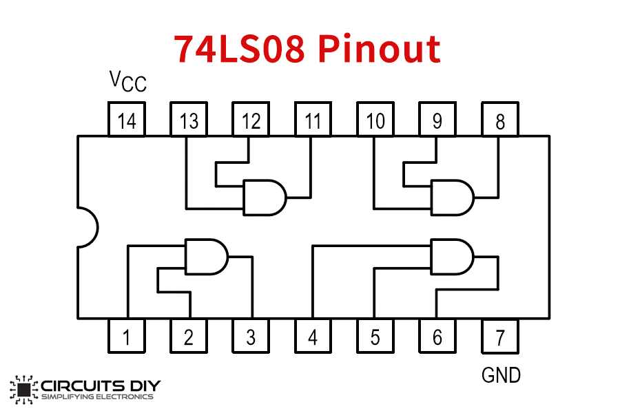
- Pins 1-3: Gate 1 (inputs 1A, 1B; output Y1)
- Pins 4-6: Gate 2 (inputs 2A, 2B; output Y2)
- Pins 8-10: Gate 3 (inputs 3A, 3B; output Y3)
- Pins 12-14: Gate 4 (inputs 4A, 4B; output Y4)
- Pin 7: GND, Pin 14: VCC
7432 — Quad 2-Input OR
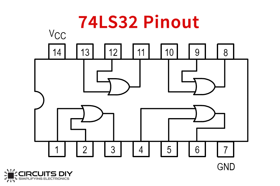
Same pinout pattern as 7408, but with OR gates instead of AND gates.
7400 — Quad 2-Input NAND
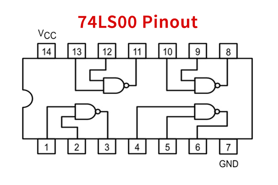
- Same physical pinout as 7408, but NAND logic instead of AND
7402 — Quad 2-Input NOR
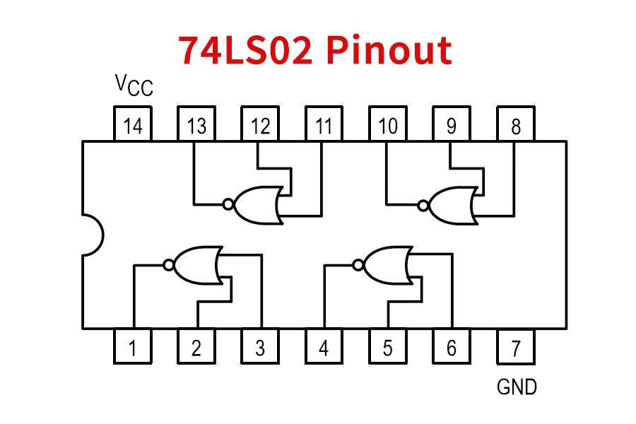
7404 — Hex Inverter
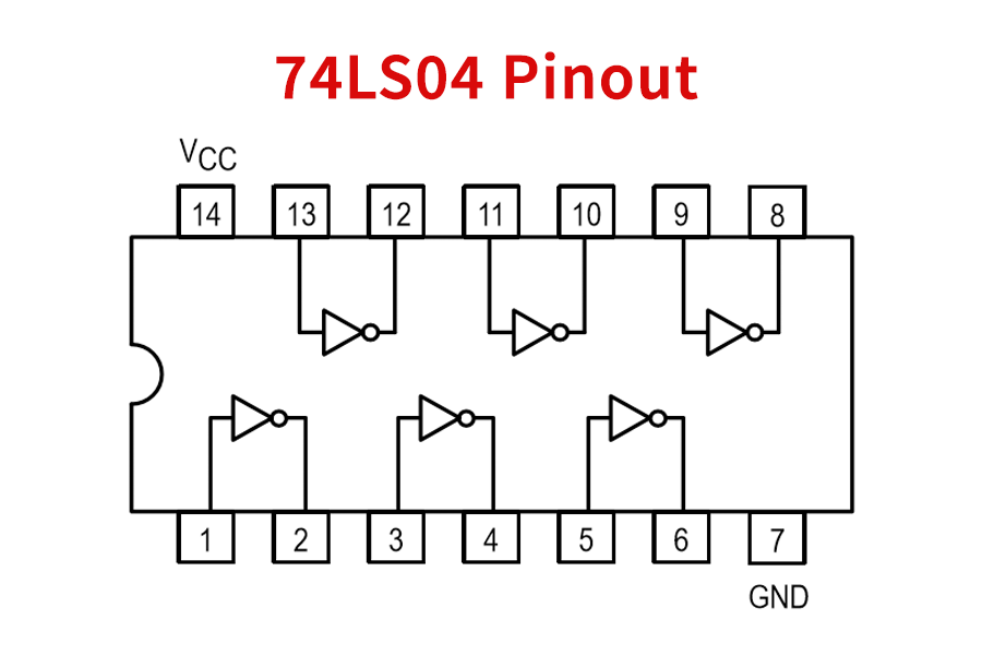
- Each inverter takes one input and produces its complement
Key insight: Always connect VCC (+5V) to Pin 14 and GND to Pin 7 on these 14-pin DIP packages. Without power, the IC won’t work. With reversed polarity, you’ll let out the magic smoke!
Part 4: Breadboard Wiring
Breadboard Anatomy
    Top Rail (+)   Top Rail (-)
    ==============  ==============
    | | | | | |    | | | | | | |   <- Power buses
    | | | | | |    | | | | | | |
    | | | | | |    | | | | | | |
    =========================================
    | | | | | |    | | | | | | |   <- Upper sockets
    | | | | | |    | | | | | | |
    | | | | | |    | | | | | | |
    | | | | | |    | | | | | | |
    | | | | | |    | | | | | | |
    =========================================
    | | | | | |    | | | | | | |   <- Lower sockets
    | | | | | |    | | | | | | | |
    | | | | | |    | | | | | | | |
    =========================================
    | | | | | |    | | | | | | |   <- Lower power
    ==============  ==============
Bottom Rail (-) Bottom Rail (+)- Horizontal rows (a-e and f-j): Vertically connected in groups of 5
- Top/bottom rails: Horizontally connected
- ICs straddle the center channel
Wiring Process for $Z = AB + CD$
Step 1: Place ICs
- 7408 (AND) for AB and CD
- 7432 (OR) for the final OR
- 7404 (inverter) if needed
Step 2: Wire power
- Connect VCC bus to +5V
- Connect GND bus to ground
- Power all ICs
Step 3: Wire the AND gates
- Input A to pin 1A of AND gate 1
- Input B to pin 1B of AND gate 1
- Output Y1 is AB
Step 4: Wire inputs C and D similarly for second AND gate
Step 5: Wire the OR gate
- Connect AB output to OR input 2A
- Connect CD output to OR input 2B
- Output Y2 is final Z
Step 6: Add input switches and output LED
Part 5: Testing Your Circuit
Testing Procedure
- Apply all LOW: Set all inputs to 0, verify output is 0
- Apply each minterm: For each row where Z = 1, verify output is 1
- Document results: Record actual outputs vs. expected outputs
Common Problems
| Problem | Possible Cause | Solution |
|---|---|---|
| Output always 0 | No power to IC | Check VCC/GND connections |
| Output always 1 | Input stuck HIGH | Check input switches |
| Wrong outputs | Wiring error | Double-check all connections |
| IC getting hot | Short circuit | Remove power immediately, check wiring |
Practice Problem — Expression to Circuit
Problem 1: Draw the logic circuit for: $Z = ABC + \overline{A}\overline{B}\overline{C}$
Show Solution
Analysis:
- Term 1: ABC (A AND B AND C)
- Term 2: $\overline{A}\overline{B}\overline{C}$ (NOT A AND NOT B AND NOT C)
- Final: OR of the two terms
Circuit:
A ----+
      (|)
      |  +-----------------+
      +--|                 |
      |  |    ____         |
B ----+--|---|    \        |
      |  |   | AND  )------+
      +--|---|____/        |
      |  |                 |   _____
      |  +-----------------|--|     \
C ----+--------------------+--| OR    )--- Z
      |                    +--|_____/
      |                    |
      |   ____             |
      +--|    \            |
         | AND  )-----------+
      +--|____/            |
      |                    |
      (|)
      |
      +--------------------+
Steps:
- Invert A, B, and C for second term
- AND A, B, C for first term
- AND $\overline{A}$, $\overline{B}$, $\overline{C}$ for second term
- OR both results
Practice Problem — Truth Table to Circuit
Problem 2: Implement the majority voting circuit (output = 1 when 2 or more inputs are 1)
| A | B | C | Z |
|---|---|---|---|
| 0 | 0 | 0 | 0 |
| 0 | 0 | 1 | 0 |
| 0 | 1 | 0 | 0 |
| 0 | 1 | 1 | 1 |
| 1 | 0 | 0 | 0 |
| 1 | 0 | 1 | 1 |
| 1 | 1 | 0 | 1 |
| 1 | 1 | 1 | 1 |
Show Solution
Step 1: Write SOP from truth table Rows where Z = 1:
- Row 3: A=0, B=1, C=1 → $\overline{A}BC$
- Row 5: A=1, B=0, C=1 → $A\overline{B}C$
- Row 6: A=1, B=1, C=0 → $AB\overline{C}$
- Row 7: A=1, B=1, C=1 → $ABC$
Expression: $$Z = \overline{A}BC + A\overline{B}C + AB\overline{C} + ABC$$
Step 2: Draw circuit
- AND gate 1: $\overline{A}$, B, C
- AND gate 2: A, $\overline{B}$, C
- AND gate 3: A, B, $\overline{C}$
- AND gate 4: A, B, C
- OR gate combines all four AND outputs
Note: This can be simplified using Boolean algebra (covered in Lesson 2.1.4) to $Z = AB + AC + BC$
Practice Problem — Using ICs
Problem 3: List the ICs needed to implement $Z = AB + CD + EF$
How many gates of each type are needed?
Show Solution
Required gates:
- AND gates: AB, CD, EF = 3 AND gates
- OR gate: combines 3 inputs = 1 OR gate
IC selection:
- 7408 (quad 2-input AND): Uses 3 of 4 gates ✓
- 7432 (quad 2-input OR): Uses 1 of 4 gates ✓
Wiring:
- 7408 Gate 1: pins 1, 2 → output pin 3 (AB)
- 7408 Gate 2: pins 4, 5 → output pin 6 (CD)
- 7408 Gate 3: pins 8, 9 → output pin 10 (EF)
- 7432 Gate 1: pins 1, 2 (from 7408 outputs) → output pin 3 (Z)
Note: For a 3-input OR, you might need to combine two 2-input OR gates, or use a different approach if a 3-input OR gate is not available.
Practice Problem — Multi-Level Circuit
Problem 4: Draw the circuit for: $Z = (AB + C)D$
Show Solution
Analysis:
- Inside parentheses: AB + C
- AB is an AND operation
-
- means OR with C
- Final: (AB + C) AND D
Circuit:
A ----+
      |   _____
B ----+--|     \
      +--| AND   )---+
      +--|_____/     |
      |              |   _____
C ------------------+--|     \
                     |  | AND   )--- Z
D ------------------+--|_____/
                     |
                     +----+
Steps:
- AND A and B → output P = AB
- OR P and C → output Q = AB + C
- AND Q and D → Z = (AB + C)D
Summary
Implementation Checklist
| Step | Action |
|---|---|
| 1 | Identify all operations in the expression |
| 2 | Draw gates for innermost operations first |
| 3 | Work outward, connecting intermediate results |
| 4 | Add inverters where needed |
| 5 | Label inputs and output |
Common ICs for AOI Logic
| IC | Gates | Use For |
|---|---|---|
| 7408 | 4× AND | Creating product terms |
| 7432 | 4× OR | Summing product terms |
| 7404 | 6× NOT | Creating complements |
| 7400 | 4× NAND | Universal gate (advanced) |
| 7402 | 4× NOR | Universal gate (advanced) |
Breadboard Rules
- ICs straddle the center channel
- Same row numbers (a-e, f-j) are connected
- Top and bottom rails are power buses
- Keep wiring organized and short
- Double-check VCC and GND before powering on
Key Reminders
- Work from the inside out when implementing expressions
- Use SOP form for AOI implementation
- Always connect VCC (pin 14) and GND (pin 7) on 74-series ICs
- One AND gate per minterm, one OR gate to combine
- Add inverters for complemented literals ($\overline{A}$ means A goes through an inverter)
- Test your circuit against the truth table row by row
- If you have unused gates, leave their inputs grounded or tied HIGH (depending on gate type)
Custom activity — adapted from PLTW Digital Electronics