Ohm Digital Electronics
1.2.4Unit 1 · Sequential Logic
Introduction to Sequential Logic: Counters
Follow the PLTW 1.2.4 activity sequence: review one D flip-flop in Multisim, build and trace a 2-bit counter, measure divide-by-two behavior, analyze a 4-bit counter, then build and verify it on hardware.
Review a Single D Flip-Flop in Multisim
Begin where the PLTW activity begins: build the single 74LS74 circuit in Multisim and test normal clocking, PRESET, and CLEAR before moving on to counters.
Your task
Do this in Multisim
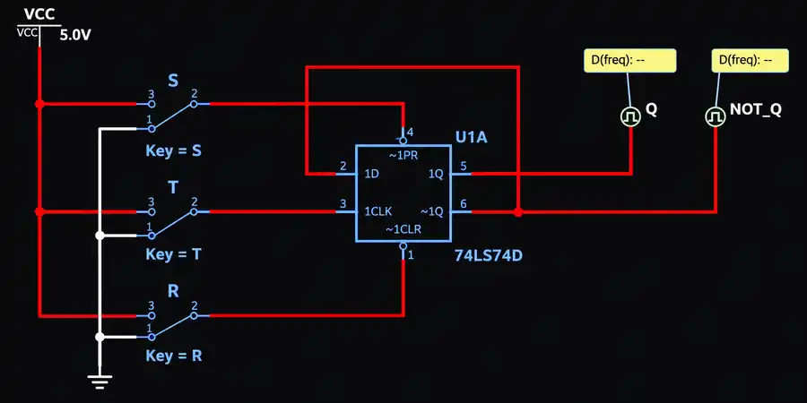
- Build the single D flip-flop circuit shown below with Q̅ fed back to D.
- Use switches S and R to set PRESET and CLEAR HIGH. Run the simulation and toggle the clock several times.
- Use switch S to set PRESET LOW and switch R to set CLEAR HIGH. Record the initial state of Q and Q̅, then toggle the clock several times and record what changes.
- Use switch S to return PRESET HIGH and switch R to set CLEAR LOW. Record the initial state of Q and Q̅, then toggle the clock several times and record what changes.
Record your flip-flop observations
Fill in each table before opening the expected-behavior reference below.
| When | Q | Q̅ |
|---|---|---|
| Initial state | ||
| Pulse 1 | ||
| Pulse 2 | ||
| Pulse 3 |
| When | Q | Q̅ |
|---|---|---|
| Initial state | ||
| Pulse 1 | ||
| Pulse 2 | ||
| Pulse 3 |
| When | Q | Q̅ |
|---|---|---|
| Initial state | ||
| Pulse 1 | ||
| Pulse 2 | ||
| Pulse 3 |
Single flip-flop screenshot
Save a screenshot of your Multisim circuit and the observed PRESET or CLEAR behavior.
Paste an image here, drop it here, or choose a file. One image is saved for this step.
D flip-flop rule
On each active clock edge, Q takes the value at D. Q̅ is the opposite of Q. Connect Q̅ to D, and Q alternates 0 → 1 → 0 on successive clock edges.
Active-LOW SET and RESET
The asynchronous SET/PRESET and RESET/CLEAR pins override the normal D/clock behavior. Keep both inactive at logic HIGH during normal counting.
Check the expected PRESET / CLEAR behavior after you test it
| PRESET | CLEAR | Expected behavior |
|---|---|---|
| HIGH | HIGH | Normal clocked operation |
| LOW | HIGH | Q forced HIGH; Q̅ LOW |
| HIGH | LOW | Q forced LOW; Q̅ HIGH |
What connection makes a D flip-flop toggle on every active clock edge?
Think about what D must be before the next clock edge if Q is supposed to become the opposite of its current state.
Connect Q̅ back to D. Q̅ is always the opposite of Q, so every clock edge loads the opposite state.
Build and Trace the 2-Bit Counter
Cascade two toggle stages and you get a binary counter. Stage A changes every clock cycle; stage B changes half as often.
2-Bit Counter Explorer
Use the pulses to rehearse the same A/B sequence you record from your Multisim circuit.
- Clock cycles
- 0
- Binary state (B A)
- 00
- Decimal
- 0
Counter reset to 00.
00The counter explorer needs JavaScript to pulse or reset. The diagram, procedure, and count sequence remain available above and below.
| Clock-In | A | B |
|---|---|---|
| Initial values | ||
| Cycle 1 | ||
| Cycle 2 | ||
| Cycle 3 | ||
| Cycle 4 | ||
| Cycle 5 | ||
| Cycle 6 | ||
| Cycle 7 | ||
| Cycle 8 | ||
| Cycle 9 |
2-bit counter screenshot
Save your Multisim counter circuit or a clear screenshot of its output sequence.
Paste an image here, drop it here, or choose a file. One image is saved for this step.
Multisim task
- Build the 2-bit counter using the dual D-type flip-flop in Multisim.
- Use a switch for Clock-In and probes for outputs A and B.
- Keep the asynchronous SET/PRESET and RESET/CLEAR inputs inactive during normal operation.
- Initialize both outputs LOW. One cycle means LOW → HIGH → LOW on Clock-In.
- Record A and B after each cycle and explain the pattern you observe.
A is the least-significant bit. To read the number normally, write the state as B A.
The current 2-bit state is B A = 10. What state should come after one more complete clock cycle?
Read B A as a two-bit binary number. The counter advances by one each cycle.
11. The sequence is 00 → 01 → 10 → 11 → 00.
Measure Clock-In, A, and B
A ripple counter is also a frequency divider. Every flip-flop stage toggles once for every two cycles of the signal driving it.
Oscilloscope setup from the activity
- Replace the manual switch with a CLOCK_VOLTAGE.
- Set it to 5 V, 50% duty cycle, 60 Hz.
- Display Clock-In, A, and B on the oscilloscope.
- Set the oscilloscope time-base to 20 ms/div and each channel vertical scale to 10 V/div. Adjust Y positions so all three traces are visible.
- Measure period with the cursors first, then calculate frequency with
f = 1/T.
| Signal | Period | Frequency |
|---|---|---|
| Clock-In | ||
| B | ||
| A |
Oscilloscope screenshot
Save the Clock-In, A, and B traces you measured in Multisim.
Paste an image here, drop it here, or choose a file. One image is saved for this step.
Check the ideal divide-by-two relationship after measuring
With a 60 Hz input, the ideal frequencies are 30 Hz at the first divide-by-two stage and 15 Hz at the next; their periods double correspondingly.
Why every stage divides frequency by two
A toggle flip-flop changes state on each active edge, so it needs two input events to return to the same state. That makes one full output period take two periods of the signal driving that stage.
If a toggle stage is driven by 200 Hz, what frequency appears at its Q output?
One toggle stage is a divide-by-two circuit.
100 Hz. Each stage halves frequency and doubles period.
Analyze and Run the 4-Bit Counter
Four toggle stages create sixteen unique states: 0000 through 1111. The same divide-by-two rule lets you predict every output frequency before you ever run the simulation.
4-Bit Binary Counter
Use this only as a visual check after you analyze the 1 kHz counter and run the PLTW Multisim version.
- Clock cycles
- 0
- Binary state (D C B A)
- 0000
- Decimal
- 0
Counter reset to 0000.
The counter explorer needs JavaScript to pulse or reset. The frequency table and binary reference remain available.
Analyze, then simulate
Analyze the 1000 Hz counter before simulating it
Start with a 1000 Hz Clock-In. Each stage halves the frequency and doubles the period.
| Signal | Period | Frequency |
|---|---|---|
| Clock-In | 1000 Hz | |
| D | ||
| C | ||
| B | ||
| A |
Check the ideal values after completing the table
For an ideal 1 kHz input: A = 500 Hz, B = 250 Hz, C = 125 Hz, and D = 62.5 Hz; the period doubles at each stage.
4-bit counter screenshot
Save your Multisim circuit or its completed 0000–1111 sequence.
Paste an image here, drop it here, or choose a file. One image is saved for this step.
Binary count reference: 0 through 15
0 = 00004 = 01008 = 100012 = 1100 1 = 00015 = 01019 = 100113 = 1101 2 = 00106 = 011010 = 101014 = 1110 3 = 00117 = 011111 = 101115 = 1111 What is the highest unsigned value a 5-bit counter can represent?
An n-bit counter has 2ⁿ unique states, starting at zero.
A 5-bit counter has 2⁵ = 32 states, numbered 0 through 31.
Build and Verify the Hardware Counter
The simulation proves the logic. The breadboard proves that you can translate the logic into real pin-level wiring and troubleshoot the result.
Build the PLTW 4-bit counter
- Use the 74LS74 datasheet pin diagram to build the four-flip-flop counter on the breadboard using two 74LS74 packages.
- Wire the four counter outputs to Y3, Y2, Y1, Y0 in descending binary order.
- Connect DIO3 to the clock input of the first flip-flop.
- Open the NI ELVISmx Instrument Launcher and select DigOut.
- Set Lines to Write: 0–3, Pattern: Ramp 0–15, and enable continuous running.
- Run the Digital Writer and verify the four outputs count in binary. Faster digital outputs can be explored after the DIO3 version works.
- Have the instructor verify the finished counter.
| Symptom | Check |
|---|---|
| Nothing changes | Check VCC/GND, the clock source, and whether PRE/CLR pins are accidentally asserted. |
| One bit is stuck | Check that stage's D-to-Q̅ feedback and its output/clock wiring. |
| The sequence skips | Check which complementary output drives the next stage and verify the correct clock-edge behavior for your device. |
| It works in Multisim but not on hardware | Re-check the actual datasheet pin numbers instead of copying symbolic pin positions from the simulator. |
Required evidence
Insert a clear image of your completed breadboarded counter into the response document assigned by your teacher. The photo should make the IC orientation, clock connection, and four output connections visible.
Completed breadboard photo
Save a clear image that shows IC orientation, the clock connection, and all four output connections.
Paste an image here, drop it here, or choose a file. One image is saved for this step.
Conclusion
- Explain why these 2-bit and 4-bit circuits are called divide-by-two counters. Connect the physical order of the flip-flops to binary place value.
- If a fifth bit were added, what would be the highest number the counter could represent? Explain how you know.
- Identify 3–5 everyday products that could contain a counter and state what each one might count.
Why does stage B represent a higher binary place value than stage A?
Stage B changes half as often as A. A completes the 1s-place pattern first; B advances only after A completes its two-state cycle, so B represents the 2s place.
Activity reference
Learning objectives
- Explain how a D flip-flop stores one bit and becomes a toggle stage when D is connected to Q̅.
- Trace a 2-bit ripple counter through its binary state sequence.
- Determine the frequency and period of each stage in a divide-by-two counter.
- Build and troubleshoot a 4-bit counter using dual D-type flip-flop ICs.
Vocabulary
- Sequential Logic
- Logic whose output depends on the present inputs and on stored past state.
- D Flip-Flop
- A one-bit memory element that copies D to Q on its active clock edge.
- Ripple Counter
- A counter where each flip-flop stage is clocked by the preceding stage rather than by one common clock.
- Frequency Divider
- A circuit whose output frequency is a fraction of its input frequency. Each toggle stage divides by two.
- Active LOW
- An input that performs its function when held at logic 0. A bar over a signal name indicates active LOW.